Kawasaki Develops Laser Patterning System for Thin-Film Photovoltaic Solar Cell Production Lines
Nov. 29, 2011
Tokyo, December 1, 2011 ― Kawasaki Heavy Industries, Ltd. announced today that it has developed a laser patterning system to be used mainly for the manufacture of thin-film solar cells.
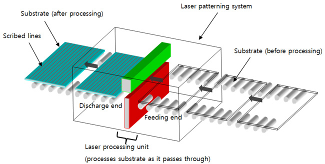
Thin-film solar cells consist of layers of films such as the transparent electrode film, semiconductor film, and metal film stacked over the surface of a glass substrate. In the process of stacking each layer of film, a patterning system is used to scribe grooves that form a circuit.
The patterning system currently in use has a processing speed of 2,000 mm/sec, and demand is high for a system capable of processing at higher speeds to help reduce the cost of solar cells. Refining the quality of the scribed lines is another challenge that needs to be addressed to achieve a higher power-generating efficiency.
The latest system developed by Kawasaki features a special laser processing unit and conveyor, enabling high-speed, continuous processing of glass substrates.
Compared with the conventional scribing method in which glass substrates are stopped, then moved back and forth as the laser is irradiated, the new system scribes faster and more efficiently and also cuts finer grooves.
High speed processing
With a maximum processing speed of 10,000 to 20,000 mm/sec, which is 10 to 20 times faster than the conventional processing method, the new system will dramatically reduce the time it takes to process a sheet of glass substrate.
Pass-through type panel feeding mechanism
By feeding glass substrates in a continuous flow and processing them at high speed, the new system reduces takt time and also makes it easier to be incorporated into the production line.
High quality scribed lines
The new system is capable of scribing smooth grooves with uniform width, keeping irregularities and burrs at a minimum. With its high-quality scribing capability, the system enables solar cell manufacturers to minimize non-generating areas and improve power-generating efficiency.
Photovoltaic power generation has been adopted by regular home-owners as well as the utility industry, and now it is also being used in what is called mega-solar power plants for large-scale power generation. This is a field on an upward trend, and the thin-film silicon type and compound-based solar cells which Kawasaki focuses on are also expected to see significant growth in the future.
Kawasaki's next step will be to combine the newly developed laser patterning system with the high pressure waterjet cleaner already on the market and offer them as apackage.
The new system will be exhibited at PVJapan 2011, which will be held at Makuhari Messe from December 5 to 7.
Kawasaki will continue to focus on developing and providing high-quality, high-performance products for the solar cell manufacturing equipment market.
Specifications of the laser patterning system
Supported substrates |
Thin-film silicon solar cell: transparent electrode film, silicon film, metal filmCIGS (compound-based) solar cell: metal electrode film |
Maximum substrate size |
1,400 mm x 1,100 mm |
External dimensions(L x W x H) |
3,500 mm x 2,300 mm x 1,500 mm |
Scribing speed |
10,000 - 20,000 mm/sec |
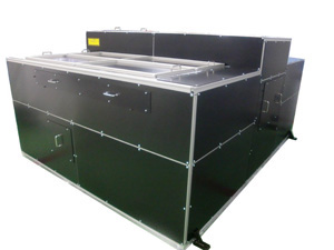
Laser patterning system image